Small Hardware Description Language
Tutorial | Navodila
This is a brief presentation of online digital circuit design educational tool with SHDL, a hardware description language based on simplified VHDL syntax. The tool is used to design small digital circuit models in a web browser, simulate the models with a graphical test bench and automatically convert to synthesizable VHDL.
Modeling and simulation in 3 steps
| 1. New Model | 2. Model Parsing | 3. Simulation |
|---|---|---|
 |  |  |
1. Circuit model and signals
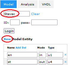
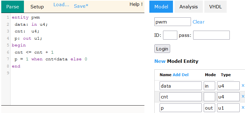
A digital circuit model is described in simplified language SHDL. The model consists of entity name, signal declarations and statement block between begin in end. An example of 4-bit counter with count enable (en):
entity counter
en: in u1
cnt: out u4
begin
if (en) then
cnt <= cnt + 1
end
end
- External circuit ports are declared using in our out mode keyword and data type. For internal circuit signals we define only data type. Signals with the same mode and type can be declared as a list.
- a,b,c: in u4
- Data type declaration includes letter u (unsigned) or s (signed) and number of bits between 1 and 64.
- u1 is one bit, u4 is 4-bit unsigned and s8 is 8-bit signed signal
- Initial value of signals can be assigned during declaration. The assigned constant notations can be decimal (5), hexadecimal (0x5) or binary ("0101" or 0b0101).
- cnt: out u4 = 1
- An array of vectors is declared with by writing the number of elements before letter u or s.
- 10u4 is an array of ten 4-bit unsigned vectors
- Enumerated data type used for FSM modeling is declared as a list of identifiers.
- state: (idle, run, stop);
Design tips
- Begin describing the circut by setting circuit name and filling the model ports and signals table. Then click on New Model Entity and the tool will generate circuit model declarations in the input editor. Exceptions are array and enumerated data types, which can not be declared in the model table.
- After parsing the model, the table header changes to Wave Ports & Signals and the table data defines simulation waveform signals.
- Before creating a new model, the SHDL code and the contents of the table can be reset by clicking on Clear.
The statement block contains signal assignment and conditional statements in simplified VHDL syntax. Statements present parts of a digital circuit operating in parallel (e.g. concurrent data-flow operations). The SHDL modeling rules:
- A statement block has one or more statements separated by a new line or semicolon.
- An assignment operator
=describes combinational logic. A set of VHDL-like operators is used for describing assigned expressions:- unary: -x, not x
- arithmetic: a + b, a - b, a * b
- logic: a and b, a or b, a xor
- concatenation and slicing: a & b, a(0), b(3:0)
- The operator
<=describes sequential logic, where the assignment is executed on rising edge of the clock. There is only one clock signal in the model, which is automatically inferred when using sequential assignments (you should not define clk in circuit ports). - Compact conditional expressions are: when...else assignment or if statement written in a single line:
sig = expression1 when condition else expression2;
if (condition) statement; - Conditional statements include a statement block after then and optional else. The statement ends with
the reserved word end, e.g.:
if condition then statement block end - Consecutive (priority) conditions can be described using elsif, similar to VHDL syntax.
- Inside a statement block is allowed only one assignment to individual singnal!
- The signal assignment statement order inside the statement block is not important.
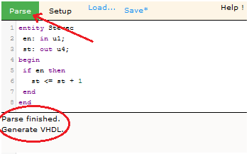
2. Model parsing
A click to Parse starts model analysis, parsing and transformation. The parser messages appear below the code editor. Successful parsing produces a message "Parse finished.", otherwise the error description appears.
Example: the code line cnt >= cnt + 1 outputs error:
Parse Error at 6:12: Expecting '='!
with information about error location (line 6, character 12) and description that the compiler expects
assignment operator.
The circuit model is transformed into internal descriprion presented in Analysis tab. Summary of the parsed circuit model resource estimation is available there. The model transformed to VHDL can be found in the VHDL tab. A click to copy is used to select and copy the generated code to clipboard for an easy transfer to external VHDL-based tools.
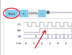
3. Simulation
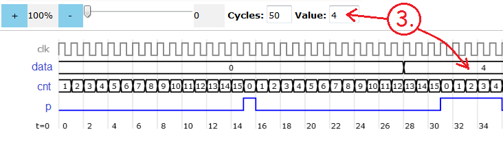
Parsing the model updates the simulation waveform with the signals from the model table. To prepare simulation, you have to enter the number of clock cycles and set the input signals. By clicking on the waveform of an one-bit input signal, the signal value toggles between zero and one. Multi-bit input signals are set to a given integer value by entering value into the form and clicking on the waveform.
The simulation is executed with a click on Run and we can immediately observe the resulting waveform. If you click Run next time, the simulation executes again, but this time starting from the last state of the circuit (this is important for sequential circuits). In order to start simulation from the reset state, you have to parse the model again and then click on Run.
Simulation tips
- Click on the input signal name to toggle the signal value in all cycles.
- Click on a signal with the right mouse button to change the waveform display from integer to binary, from binary to analog and from analog back to integer.
- Check autoinc to increment input values when setting vector signals.
Circuit model analysis
The SHDL tool preforms analysis of the described circuit model. Reports accesible at the tab Analysis include: parsed model code (Visit), estimated circuit area (Resources) and circuit data-flow graph (DFG). Resource summary presents the number of input-output pins, flip-flops, logic, arithmetic and comparisson operators, and multiplexers.
The circuit area is estimated by decomposing the circuit into a data-flow graph and evaluating graph nodes as circuit building blocks. The reported building blocks (eg. mux, cmp, add) area is based on evaluation of syntesized circuits in CMOS technology. The esimated ASIC circuit area is sum of building blocks areas normalized to the size of a standard 2-input NAND2 gate and divided into combinational and sequential (flip-flop) circuit parts. The expected sinthesized circuit area is usually smaller, due to the optimization, but the SHDL estimation is still useful as a guide to compare various circuit models.
Example: Analysis of an 8-bit modulo counter.
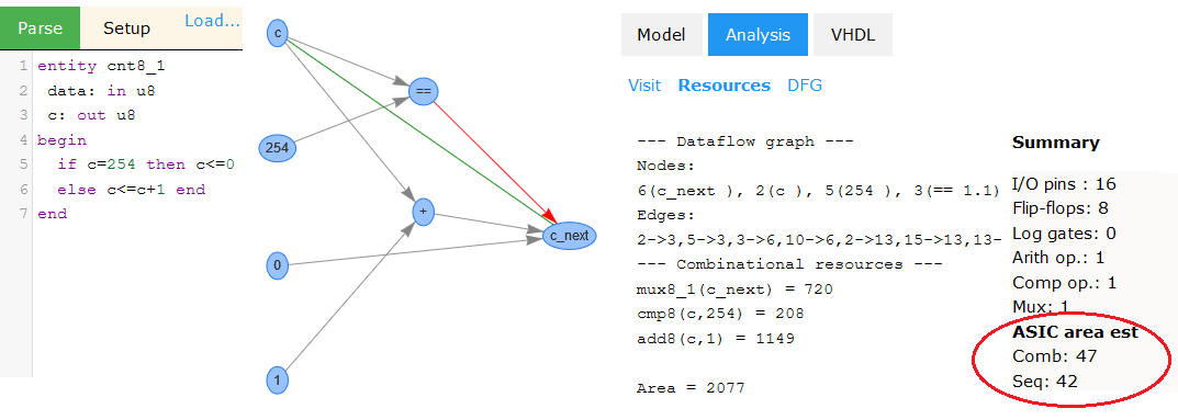
The counter circuit consists of an 8-bit multiplexer (mux8), a comparator (cmp8) and an adder (add8). Total estimated combinatinal logic area is 47 standard NAND2 gates and sequential area is 42 NAND2 gates.
Additional features
The SHDL tool is regularly updated with additional features, for example interactive virtual board support.