[LNIV Red Pitaya](index.html)
# 1. [Red Pitaya](https://www.redpitaya.com/) signal processing: scaling & averaging
The tutorial presents how to upgrade the [Red Pitaya project Classic](redpitaya-classic.htm) with a custom signal
processing component in VHDL. The classic project includes peripheral modules for housekeeping, digital oscilloscope, arbitrary signal generator ASG and PID regulator. The rarely used module PID, which is connected to both input and output
analog channels, will be replaced by the custom component.
The component **proc** is connected to ADC or signal generator input channels and DAC output channels. The processing
system controls the component through a simple system bus (sys[3]).

A digital_loop control signal from the housekeeping component is used to control signal path of the component **proc**. Setting digital_loop to 1 connects its inputs (dat_a_i, dat_b_i) to ASG and outputs (dat_a_o, dat_b_o) to
the scope component. The **proc** outputs are also connected to external DAC.
The first part of the tutorial presents project setup and implementation of data scaling: input channels are
amplified or attenuated by a scaling factor set is software.
## Vivado project
We begin with preparing the Red Pitaya Classic project in Vivado 2019 using ZIP archive and build scripts.
- Unzip the archive: [redpitaya-classic.zip](https://lniv.fe.uni-lj.si/courses/div/redpitaya-classic.zip)
into your project folder. The SystemVerilog source files are located in rtl subfolder.
- Run Xilinx Vivado, navigate to the project folder using TCL console and run the script:
```
cd c:/proj/redpitaja
source ./make_project.tcl
```
- The script creates a new Vivado project, block design and includes source files. The Vivado project file is located inside **project** folder.
- Edit the top level source **red_pitaya_top.sv** and replace declaration of **pid_dat** with **proc_i** and **proc_o** (line 160):
```
SBA_T [2-1:0] proc_i;
SBA_T [2-1:0] proc_o;
```
- To describe input multiplexers check the code in line 340. Change the existing assignments to
**adc_dat** and write new assignments to **proc_i**. Change also the **dac_a_sum** and **dac_b_sum**
assignment:
```
assign adc_dat[0] = digital_loop ? proc_o[0] : {adc_dat_raw[0][14-1], ~adc_dat_raw[0][14-2:0]};
assign adc_dat[1] = digital_loop ? proc_o[1] : {adc_dat_raw[1][14-1], ~adc_dat_raw[1][14-2:0]};
assign proc_i[0] = digital_loop ? asg_dat[0] : {adc_dat_raw[0][14-1], ~adc_dat_raw[0][14-2:0]};
assign proc_i[1] = digital_loop ? asg_dat[1] : {adc_dat_raw[1][14-1], ~adc_dat_raw[1][14-2:0]};
assign dac_a_sum = proc_o[0];
assign dac_b_sum = proc_o[1];
```
- Replace the **red_pitaya_pid** with component named **proc**. The code at the end of the **red_pitaya_top.sv** source shold change to:
```
proc i_proc (
// signals
.clk_i (adc_clk ), // clock
.rstn_i (adc_rstn ), // reset - active low
.dat_a_i (proc_i[0]), // in 1 from ADC or loopback
.dat_b_i (proc_i[1]), // in 2 from ASG
.dat_a_o (proc_o[0]), // out 1
.dat_b_o (proc_o[1]), // out 2
// System bus
.sys_addr (sys[3].addr ),
.sys_wdata (sys[3].wdata),
.sys_wen (sys[3].wen ),
.sys_ren (sys[3].ren ),
.sys_rdata (sys[3].rdata),
.sys_err (sys[3].err ),
.sys_ack (sys[3].ack )
);
```
- Add file [proc.vhd](proc1.vhd) to the project. The component includes
system interface with ID, two 8-bit registers and logic for input data scaling. The register addresses start at
0x01000 to avoid conflict with assigned PID address spaces in web applications (e.g. the scope application has
no info that we replaced PID and continuously sets some PID registers). The data scaling is described as multiplication
of the inputs with register **a** or **b** values, cropping and shifting the results bits (divide by 16). The operation
effectively performs scaling with fixed point values in 4.4 format:
```
-- multiply signed inputs with 8-bit register, register values are unsigned
mul_a <= signed(dat_a_i) * signed('0' & a);
mul_b <= signed(dat_b_i) * signed('0' & b);
-- divide by 16 (multiplication format 4.4), possible output overflow
dat_a_o <= std_logic_vector(mul_a(17 downto 4));
dat_b_o <= std_logic_vector(mul_b(17 downto 4));
```
- Start Vivado compilation (Run Implementation, Generate Bitstream) and locate the output file
red_pitaya_top.bit in a folder project\redpitaya.runs\impl_1.
## Simulation
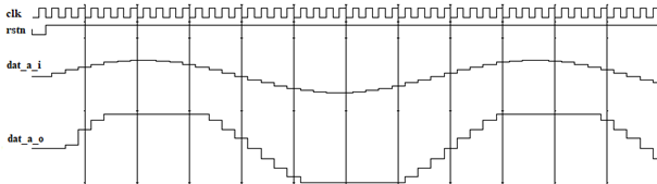
Signal processing component should be verified with simulation using provided test bench
[tb_proc.vhd](tb_proc.vhd). The testbench generates control signals (clk_i, rstn_i), simulates system
bus transactions to set registers and produces sine waveform on the signal input.
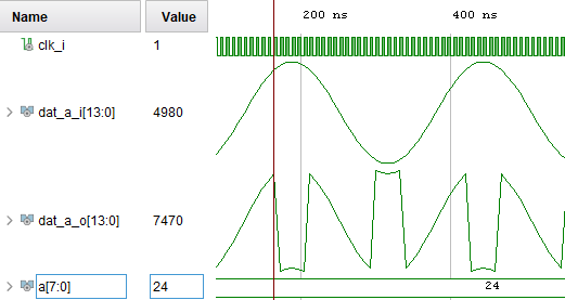
Example simulation waveform shows the input and output signals when scaling is set to 24/16 = 1,5.
The output is amplified and overflow occures at the peak sine values.
### Excercise: saturation and averaging logic
You can add saturation logic to the processing component, which should behave like analog amplifier. If the multiplied data is out of 14-bit range (-8192 to 8191), the output should be saturated to positive or negative limit:
You can also add 4 consecutive registers in the input signal path and summarize register values to obtain a data
averaging circuit. Data averaging operates as a low-pass filter.
## Upload to STEMlab
- Connect STEMlab to local internet router and use SFTP tool (for example [Bitvise SSH Client](https://www.bitvise.com/ssh-client) to upload the bitstream file in the board local folder (root).
- Change the ScopeGen application setting to use this file by writing the path to the bitstream in:
```/opt/redpitaya/www/apps/scopegenpro/fpga.conf```).
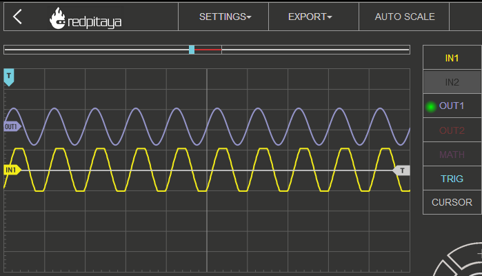
- Open Red Pitaya in your web browser and run Oscilloscope. Set one signal generator output by clicking on the wheel near
OUT1 and selecting ON. The scope will show a sine wave. Now test the bitstream version by reading the address 0x40301000
which should return the ID (FE020210) and set the digial loopback by writing in a terminal:
```
monitor 0x40301000
monitor 0x4000000c 1
```
- Test the signal scaling by setting different values to the address 0x40301004, for examle:
```
monitor 0x40301004 24
```
- The ASG test signal can be amplified or attenuated depending on the scaling settings. An overflow can occur
due to cropping the multiplication signal to 14-bits. With additional code in proc.vhd you can detect overflow
and make saturated output.
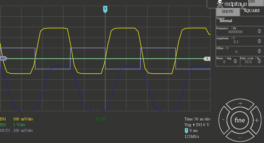
If you set the input to a sqaure waveform, you can observe data averaging function. The set frequency is 6 MHz,
a yellow signal is result of scaling with loopback and the blue waveform adds averaging.