[LNIV Red Pitaya](index.html)
# 2. [Red Pitaya](https://www.redpitaya.com/) signal processing: numerical oscillator
This tutorial presents development of a numerically controlled oscillator (osc) on the Red Pitaya STEMlab board.
The osc component (Verilog module) will be included to the [Red Pitaya Classic project](redpitaya-classic.htm) by
replacing PID component. Scope with the associated application in used for observing generated signals.
## Vivado 2019 Project
- Unzip the project from: [redpitaya-classic.zip](https://lniv.fe.uni-lj.si/courses/div/redpitaya-classic.zip),
open Vivado and run TCL script:
```
cd c:/proj/redpitaja
source ./make_project.tcl
```
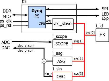
- Edit top-level file: red_pitaya_top.sv, search for assignment of dac_a_sum. Replace the existing adder
assignment with the code:
```
wire [13:0] sin_o
assign dac_a_sum = asg_dat[0] + sin_o;
```
- at the end of the top-level file change red_pitaya_pid to red_pitaya_osc
and write appropriate connections:
```
red_pitaya_osc i_sin (
.clk_i (adc_clk ), //clock
.rstn_i (adc_rstn ), //negative reset
.sin_o (sin_o ), //14-bit sine output
.addr_i (sys[3].addr ), //32-bit address
.wdata_i (sys[3].wdata), //32-bit write data
.wen_i (sys[3].wen ), //enable write
.ren_i (sys[3].ren ), //enable read
.rdata_o (sys[3].rdata), //32-bit read data
.err_o (sys[3].err ), //bus error
.ack_o (sys[3].ack ) //acknowledge
);
```
## Numerically Controlled Oscillator
NCO consists of a system bus interface, a phase counter (cnt) and sample ROM used for the output waveform.
The ROM address inputs are connected to the upper 10 bits of the phase counter.
The 24-bit counter adds at each clock cycle (125 MHz) a value from the register (reg).
Output signal frequency depends on the set register value.

The system bus interface enables writing and reading the registers in the module.
The peripheral address space is divided into blocks,
so only lower 20 bits of the address are decoded. For the exercise, you can add aplitude and offset setting registers.
### Verilog module and simulation
The basic module of the numerically controlled oscillator: [red_pitaya_osc.v](osc/red_pitaya_osc.v)
Memory model containing 256 samples of 10 bit sine signal: [rom.v](osc/rom.v)
```Verilog
always @(posedge clk_i)
begin
if (~rstn_i) begin
register <= 32'h00000000;
cnt <= 24'h000000;
end else begin
cnt <= cnt + register[23:0];
if (wen_i && (addr_i[19:0]==20'h10004)) begin
register <= wdata_i;
end
end
end
assign rom_addr = cnt[23:16];
rom u0(.adr(rom_addr), .data(rom_data));
assign data_o = rom_data;
```
Interface consists of logic for reading module ID and register and writing to the register. The register offset address
should be above the addresses reserved in the classic project to avoid conflicts with applications which try to initialize
some PID registers. Reading any other address returns the circuit ID (FE002020).
- Verify the operation of the sine generator with a testbench [test_osc.v](osc/test_osc.v) which should set the register
to the value 10000.
### VHDL component and simulation
Description of the oscillator wit system bus interface: [red_pitaya_osc.vhd](osc/red_pitaya_osc.vhd)
Generic ROM with 1024 samples of 10-bit sine waveform: [rom.vhd](osc/rom.vhd)
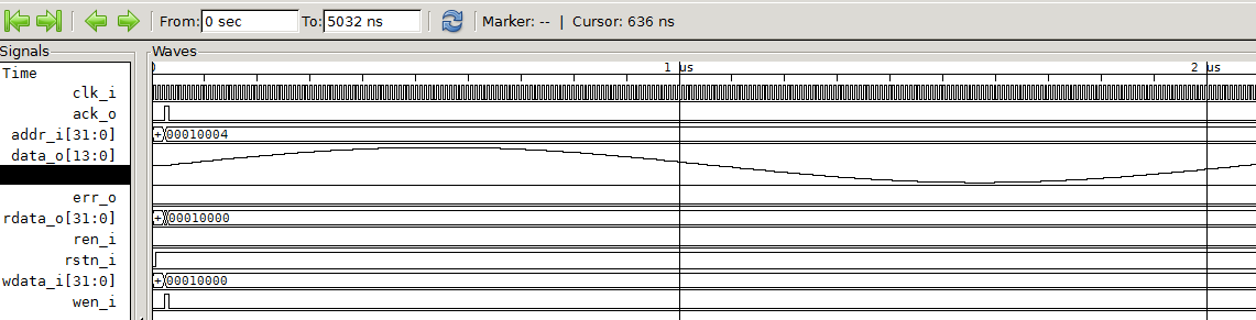
- Verify the operation of the sine generator with a testbench [osc_tb.vhd](osc/osc_tb.vhd) which should set the register
to the value 10000. Use Vivado simulator or open-source simulator [GHDL](http://ghdl.free.fr/) with additional Waveform viewer
[GTKWave](http://gtkwave.sourceforge.net/). Instructions for compiling in GHDL and running simulation:
```
ghdl -a rom.vhd
ghdl -a red_pitaya_osc.vhd
ghdl -a osc_tb.vhd
ghdl -r osc_tb --stop-time=2000ns --vcd=osc.vcd
```
Simulation result:
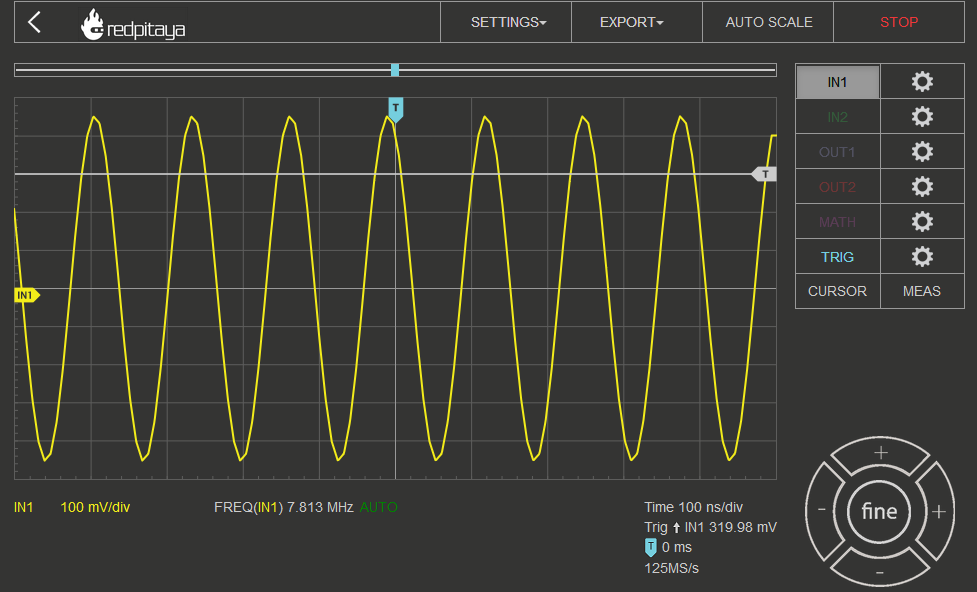
## Test on STEMlab
After implementation of the digital system in Vivado and generating bitstream file red_pitaya_top.bit, transfer the file
to the STEMlab. The operation of the numerical oscillator can be observed with the scope application. First you should
set the application associated bitstream to the new file. The file path is described in:
*/opt/redpitaya/www/apps/scopegenpro/fpga.conf*.
When you click on the Oscilloscope & Signal Generator application, the bitstream is loadded to the FPGA. You can
check this by reading ID in the terminal:
```
monitor 0x40300000
```
which should return value FE002020. Now set the increment of the numerical oscillator:
```
monitor 0x40310004 100
```
and observe the generated waveform: